

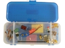
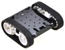
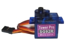
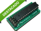
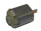
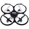
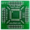
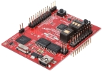
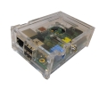
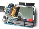
Productos Destacados


 Facebook
 Twitter
 Linkedin
 Youtube
LO MAS VENDIDO


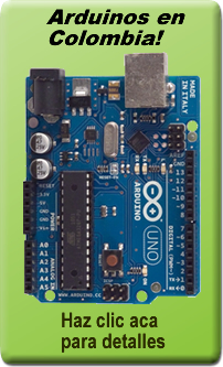
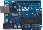
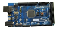
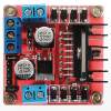
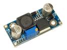
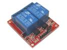
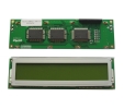
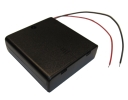
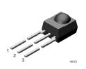
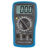
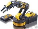
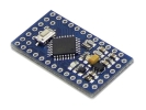
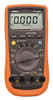
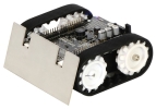
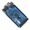
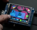
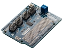
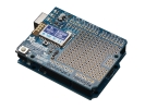
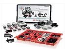
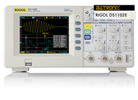
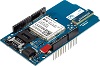
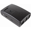
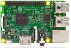
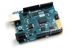
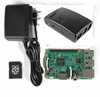
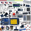
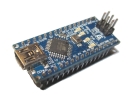
| Curso Seminario online de Arduino español electronica practica robotica basica con Arduino Bogota tutoriales gratis entrenamiento capacitacion estudiantes colegios profesores niños jovenes hobistas aprendiendo Diplomado online Arduino Internet como aprender curso de electronica videotutoriales practicas enseñanza laboratorios makers diseñadores Arduino desde Cero Donde aprender Arduino por Internet Raspberry Pi Lego TIC tecnología Colombia programacion Microcontroladores Atmel Almacenes electronicos Carrera novena 9na Bogota Almacen Electrónica tienda de partes electronicas Sigmaelectronica teckcien lared la Red electronica electronica de la 55 Tienda de Robotica Laboratorio de ingeniería electrónica LabCenter Micropicplus Semiconix Betacolor Plintec AVS Medellin Compuvideo Barranquilla Importronic S.A. Pereira Equipos de medida amplificadores equipos electróncicos repuestos electrónicos instrumentación importaciones. Nuestro... Audio Video Pereira Articulos Electronicos Almacén Electro Frío Cartagena Electronica Cartagena Electrovisión Ltda Manizales Equipo electrico Manizales Electronica Manizales Manizales Muzca Technology Envigado Wifi ingenieria y desarrollo de producto zigbee robótica gsm rfid microcontroladores motores componentes Articulos Electronicos Medellin Componentes electronicos Medellin Electronica Medellin Electromoto Ind. Tony Bucaramanga Dynamoelectronics C & C Electronica Cali Electrónica La Pava Buga Equipo electrico Buga Electronica Buga Componentes electronicos Buga Soni video Bogota Componentes electronicos Bogota Electronica Medellin Componentes electronicos Medellin Sonido Suconel Medellin Didacticas electronicas Punto Electrónico Neiva Componentes electronicos Neiva Electronica Neiva Electrónica Shalom Barranquilla Componentes electronicos Barranquilla Electronica Barranquilla a Ingenieria electronica Cartagena Electronica Cartagena Equipo de audio Cartagena Electrónica Montería Equipo de sonido Monteria Instrumentos medicion Monteria Almacén Electro Philips Neiva Electronica Neiva Componentes electronicos Neiva Sonido Neiva Sonido Electrónico Sincelejo Instrumentos medicion Sincelejo Venta de instrumentos Sincelejo Componentes electronicos Sincelejo Audio y Video Sincelejo Discos Sincelejo Instrumentos musicales Sincelejo Sonytécnicos Acacias Electrodomesticos Acacias Equipo de sonido Acacias Componentes electronicos Acacias Compu-electrónica I.a. San Gil Componentes electronicos San Gil Electronica San Gil Reparar Electrónica Puerto Berrio Electronica Puerto Berrio Equipo de sonido Puerto Berrio Video Puerto Berrio Mundo Electrónico Villavicencio Articulos Electronicos Villavicencio Reparacion Villavicencio Electrodomesticos Villavicencio Cca Electrónica Ipiales Componentes electronicos Ipiales Electronica Ipiales Poder Electrónico Bucacentro Bucaramanga Articulos Electronicos Bucaramanga Televisores Bucaramanga Componentes electronicos Bucaramanga Multi Electrónica Bucaramanga Componentes electronicos Bucaramanga Electronica Bucaramanga Punto Electrónico Monteria Reparacion Monteria Articulos Electronicos Monteria Berdugo Faustino Barranquilla Componentes electronicos Barranquilla Electronica Barranquilla Ar Semiconductores Barranquilla Electronica Barranquilla Componentes electronicos Barranquilla Almacén Pepe Visión Barranquilla Electronica Barranquilla Componentes electronicos Barranquilla Selectron 2000 Equipo electrico Soni video Manizales Electrodomesticos Manizales Televisores Manizales Componentes electronicos Manizales Almacén y Servicio eléctrico Willard De Nariño Atahualpa Pasto Componentes electronicos Pasto Electronica Pasto Kautin Jd Electronic Santa Marta Electronica Santa Marta Componentes electronicos Santa Marta Almacén Surtielectrónica Manizales Computadores Manizales Computacion accesorios Manizales Electronica Manizales |